Announcement

Collapse
No announcement yet.

Concept Design

Collapse
X
 
  • Filter
  • Time
  • Show
Clear All
new posts

  • I can see 2 possible gotchas:

    1) the sampling clock and the signal are harmonically correlated
    Easy to solve. We can change signal frequency (or sampling clock) to avoid this.

    2) input signal amplitude is smaller than q / 2 , (LSB is also often called a quantum (q)).
    I don't know if I understand this; first pick would be higher gain at RX frontend.

    Even if I am completelly missunderstanding this; still worth to consider it.
    Too many good specs to toss it like that.
    And by the price you simply can't resist!


    And it is Arduino supported too! Wow!
    I checked IAR​ Embedded Workbench too.
    Those Nucleo boards are very well supported and covered.

    Comment


    • Hi first time posting here.
      I found this forum last week and am following along with great interest, also the MAGPI project.
      I am completely new to metal detecting, however have a fair bit of experience in mostly digital electronic design and embedded development.

      A thought I had pondering over the project over the last few days is that this first iteration would mainly be for forum members to build test and evaluate as opposed to a finalized ready to build and go design. Correct me if I’m wrong here.

      In such a case designing it a bit more like a dev board could have some advantages.
      Some of the ideas I had is to allow for both direct sampling and multiple integrated sampling windows on the same PCB and the possibility of logging direct sample data to an SD card.


      Adding alternative circuit options to the PCB and leaving it unpopulated should have fairly minimal drawbacks.
      However, working with a µC that can both support all the timer channels for the integrated sampling and the throughput of direct sampling to DSP and SD card could overly complicate the design.

      A benefit of an SD card would be a “standardised” way of sharing readings from in the field over a wide variety of soil types and coils. Currently it seems photos of an oscilloscope screen with the detector on the bench are the only way of doing this. This could allow for some advanced data analysis to narrow down the exact signals we are interested in and what we want to ignore.
      Having both the integrated sampling and direct ADC would allow easy experimentation of wide variety of sample windows and evaluation of which design is most effective.
      If it turns out that a handful of sampling windows with clever timing are just as effective as direct sampling a more finalized design could drop support for direct ADC possibly lowering build cost.
      Much of the above assumes that multiple analogue integration windows, are a more effective way to get very precise readings with cheaper hardware, given that the optimal window timings are well understood.


      Regards Tony

      Comment


      • Welcome Tony... "welcome to the jungle" !
        Nice proposals, I like it.
        My two Nucleo 144 devs are on the way from USA, will be here in 10 days time frame.
        Looking forward.
        I am not against direct sampling, on contrary, but objective reasons and subjective conditions forcing me to think alternative.
        Things can be done, things can be prepared and processed well, so even 12bit ADC to work the job just fine.
        Nucleo offers even 16bits with certain tradeoffs. But 5MSPS is hard to resist. 16 timers... not even to mention that!
        Last time I tried to "squeeze some juice" and run synchonized multiple pulses&pauses was with Atmega328P and only 3 timers, one 16bit and two 8bit.
        I managed to "squeeze" 3 separate pin functions like that, which works well on Barracuda kind of detector.
        But here, this project, need a lot more than that. So 16 timers are quite enough.
        I will not elaborate alternative solutions here, since nobody showed good will to even listen me, I will say only this;
        RX frontend can be configured in a way to provide already "processed" usefull parts of signal and then 12-16bit ADC will have easy task later.
        But I like your proposal, it makes a lot of sense to me.
        As I am concerned; you are very welcome to elaborate your ideas further.


        Comment


        • Originally posted by tpet93 View Post
          [FONT=Calibri
          A benefit of an SD card would be a “standardised” way of sharing readings from in the field over a wide variety of soil types and coils. Currently it seems photos of an oscilloscope screen with the detector on the bench are the only way of doing this. This could allow for some advanced data analysis to narrow down the exact signals we are interested in and what we want to ignore.
          Fully agree with this proposal.
          I personally always connect an SD card socket (with a FATS-compatible driver) on all my experimental systems .
          Using a large buffering allows the logging of fast events (down to 1msec intervals) happening during bench/field tests.
          indeed, the ASCII-coded comma-separated files can then be studid in details on EXCEL with corresponding curves.

          We have discovered that the serial link set at high baud rate (500Kbauds) can also be very useful to study the behaviour of a system in real-time using a terminal emulator with a data scope function.
          This is only available for bench tests, no field tests.

          Comment


          • Аt the risk of saying something inappropriate, but it occurred to me : the next step is the transfer of information between the smartphone and the metal detector . Тhis will allow absolutely inexperienced and incompetent operators to work with rapid learning , voice commands , quick upgrade , etc. Тhe smartphone connected to a server at the detector manufacturer company is probably the start(artificial intelligence – mandatory ) . Аfter that - maybe the SIM card in the detector and the smartphone drops out? Smartphone interference on the detector require a more special mode . Humanity has been progressively dumbing down in recent centuries and as technology advances - the more fools... Me too

            Comment


            • Originally posted by Carl-NC View Post
              Here is a first-cut at noise analysis. I will use a simplified version of Tony's front-end schematic:

              Now we need the noise bandwidth. If we assume we want to respond to a 0.25us target then we need a bandwidth of


              Hi Carl,
              I was looking at your noise analysis and the following question came to me. If we need to respond to a 0.25us target don't we need the op amp's bandwidth to be 3 times (or even better 5 times) the above calculated bandwidth?
              That will make the bandwidth 1.9MHz (3x) or 3.2MHz (5x) and then the noise will increase somewhat as well.

              Comment


              • Originally posted by lucifer View Post
                I was looking at your noise analysis and the following question came to me. If we need to respond to a 0.25us target don't we need the op amp's bandwidth to be 3 times (or even better 5 times) the above calculated bandwidth?
                That will make the bandwidth 1.9MHz (3x) or 3.2MHz (5x) and then the noise will increase somewhat as well.
                Yes, but it's a matter of variation in sensitivity rather that will detect/won't detect. In the frequency domain, setting the preamp BW to exactly the same as the target tau means that the preamp gain will be -3dB for that target, so you loose some sensitivity. If you set the BW to 3x the target tau, then the gain for that target is -1.25dB; at 5x it's -0.8dB. So, yes, increasing the BW will help. In the time domain you are convolving the target's exponential response with the preamp's exponential recovery settling so it's mathematically more complicated but the end results are similar.

                0.25us is probably a little aggressive but I chose it as a starting point for doing noise analysis because its noise BW comes out to exactly 1MHz which makes calculations a little easier. I needed something to get a first-cut idea on ADC bits, but in the final design the preamp BW can easily be changed by swapping a few caps so we can dial it in later.

                Comment


                • Not directly related to the last couple of posts... but coincidentally, I'm currently troubleshooting a problem connecting a SPI flash eeprom to an Arduino.
                  It is the Winbond 25Qxx series. There are "everywhere".
                  Old motherboards from various PCs and laptops, set top boxes, various embedded devices... are really in mass use and very easy to get hold of.
                  I have a dozen pieces that I have already removed from the old devices, and I guess I have another hundred pieces on the boards, which have not been removed yet.
                  I currently have 1, 4 and 16 Mb capacities.
                  The "problem" of connecting to Arduino UNO boards is the voltage levels.
                  The Arduino UNO is powered by 5v, so the logic on the pins is also at that level. W25Qxx is powered by 3v3 and the logic is at that level.
                  There are very few "solutions" on the internet... and as far as I've seen; most are not valid. Does not work.
                  People try to adjust the levels with resistive dividers and that is a very bad solution.
                  An alternative solution is an Arduino that works on 3v3, for example Mini and Mini Pro (and a few more).
                  But I don't want that solution, I deliberately want an Arduino UNO, for many reasons that are irrelevant here.
                  So I resorted to the only possible solution; and it is a modification of Arduino UNO to work on 3v3. It's a work in progress, I can't confirm it's the correct solution yet.
                  But the point is the following; I have worked with various SD readers and SD cards. SPI flash eeprom has many advantages. I think there is no need to list them.
                  Apart from speed and 4mA consumption in active mode; a very important reason for is the size of the chip and the place it will occupy on the pcb, as well as the ease of connection.
                  In particular, that chip will serve as "ROM" for me. The previously written database will be read-only by mcu.
                  Such are the needs of the device I work on.
                  As for the current PI detector project, I assume that the chosen development system will have sufficient resources and memory; so no additional SPI flash will be needed.
                  But if one opts for a more modest development system with less memory; I think using additional SPI flash memory is a very good idea.
                  Just... another idea to think about.
                  ...
                  I have the impression that this topic has died.
                  No one is announcing anything concrete.
                  If I was "in a hurry" in the beginning... now a lot of time has passed and now I can't be accused of wanting things too fast.
                  It is clear that this project will end up with 2-3 interested parties.
                  I'm sorry to sound pessimistic but I think it's time for a reality check.
                  I knew all this the very first day the first post was published….

                  Comment


                  • Originally posted by ivconic View Post
                    I have the impression that this topic has died.
                    No one is announcing anything concrete.
                    See the TX thread for my latest post.

                    Comment


                    • I saw part of the schematic you posted.
                      See... to understand what you posted; I would have to read the whole topic... and maybe more topics, from the beginning.
                      And to remember every little thing that someone somewhere mentioned, then to connect everything into a coherent whole.
                      Because the whole story is pretty watered down from the beginning.
                      There is nothing concrete published in its entirety with a complete explanation.
                      Now I should ask you more questions to understand the schematic.
                      For example, what is the voltage coming out of the buck regulator, what exactly are the fets, what does "Cextra" mean and what is its role there... etc.
                      What does ADC1 and ADC2 mean to you, why? What is the purpose of those two samples?
                      And so in order... part by part of the schematic that will be published further, there will always be many unfinished things that need to be explained immediately in the same post.
                      The start was wrong, in my opinion. There was a lot of idle talk, a lot of unspecified things.
                      While it was going on; a person loses the will to follow closely, loses focus and after some time what he read is no longer clear to him.
                      In this way, it is very difficult to follow a clear flow of thoughts and ideas.
                      During the week I do 50 different things that are similar and not similar to each other.
                      I don't have time to re-read a dozen topics to understand "what the writer wanted to say" with one detail in the schematic.
                      A clear "algorithm" is necessary for such a complex project. And not only to write that "algorithm"... but also to strictly follow it.
                      I don't know if you are familiar with the way it is normally done in the programming world, at least here in the EU?
                      There is a "ticketing system" with workflow such as Jira (now there are even better ones), where the author gives precise details of each step he takes on the project.
                      And the other participants in the project leave so-called "tickets" with questions, remarks and possible suggestions to change something, fix it, etc.
                      I think it should have started in that way. Devote one topic exclusively to chronology and details.
                      Of course that topic would make sense; only if other participants should not write anything but just add "tickets" as needed.
                      I don't know how it is possible to do that in this type of forum. But I don't think it's a bad idea.

                      In this way, as things stand now; we will have to (at least most of us) wait for you to make it yourself, to test it, to make everything work as you imagined,
                      to do the whole schematic, to draw the pcb, to write the whole code... and finally to publish it all. Like a finished project.
                      And if in the meantime it turns out that it turned out to be phenomenal... you change your mind, you decide to make it a commercial project and in the end you
                      keep quiet and don't publish anything concrete. And then we wasted our time here from the beginning!

                      And it's not impossible for some idiot to accuse me of wanting everything done, of wanting a super project on my plate without contributing anything myself.

                      How can I contribute anything in this way? A very awkward situation indeed!
                      The only thing left for me is to occasionally resent all this...

                      This is a game of attrition... only the most persistent will survive! I gave up a long time ago...
                      I died in the first rows at the start...

                      ​​​

                      Comment


                      • Yes, you have to read the threads if you hope to understand. If you still don't understand, then ask questions. Preferably in the relevant thread.

                        Comment


                        • True.
                          Done.

                          Comment


                          • Originally posted by ivconic View Post
                            Not directly related to the last couple of posts... but coincidentally, I'm currently troubleshooting a problem connecting a SPI flash eeprom to an Arduino.
                            It is the Winbond 25Qxx series. There are "everywhere".
                            Old motherboards from various PCs and laptops, set top boxes, various embedded devices... are really in mass use and very easy to get hold of.
                            I have a dozen pieces that I have already removed from the old devices, and I guess I have another hundred pieces on the boards, which have not been removed yet.
                            I currently have 1, 4 and 16 Mb capacities.
                            The "problem" of connecting to Arduino UNO boards is the voltage levels.
                            The Arduino UNO is powered by 5v, so the logic on the pins is also at that level. W25Qxx is powered by 3v3 and the logic is at that level.
                            There are very few "solutions" on the internet... and as far as I've seen; most are not valid. Does not work.
                            People try to adjust the levels with resistive dividers and that is a very bad solution.
                            An alternative solution is an Arduino that works on 3v3, for example Mini and Mini Pro (and a few more).
                            But I don't want that solution, I deliberately want an Arduino UNO, for many reasons that are irrelevant here.
                            So I resorted to the only possible solution; and it is a modification of Arduino UNO to work on 3v3. It's a work in progress, I can't confirm it's the correct solution yet.
                            But the point is the following; I have worked with various SD readers and SD cards. SPI flash eeprom has many advantages. I think there is no need to list them.
                            Apart from speed and 4mA consumption in active mode; a very important reason for is the size of the chip and the place it will occupy on the pcb, as well as the ease of connection.
                            In particular, that chip will serve as "ROM" for me. The previously written database will be read-only by mcu.
                            Such are the needs of the device I work on.
                            As for the current PI detector project, I assume that the chosen development system will have sufficient resources and memory; so no additional SPI flash will be needed.
                            But if one opts for a more modest development system with less memory; I think using additional SPI flash memory is a very good idea.
                            Just... another idea to think about.
                            ...
                            I have the impression that this topic has died.
                            No one is announcing anything concrete.
                            If I was "in a hurry" in the beginning... now a lot of time has passed and now I can't be accused of wanting things too fast.
                            It is clear that this project will end up with 2-3 interested parties.
                            I'm sorry to sound pessimistic but I think it's time for a reality check.
                            I knew all this the very first day the first post was published….
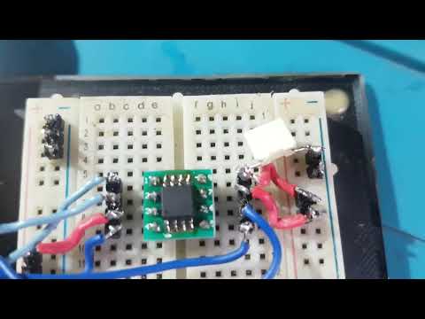
                            Total success!
                            Modded Arduino UNO now works at 3v3, LCD and keyboard at 5v.
                            I put 1 sec delay between readings, for testing purposes.


                            Comment

                            Working...
                            X