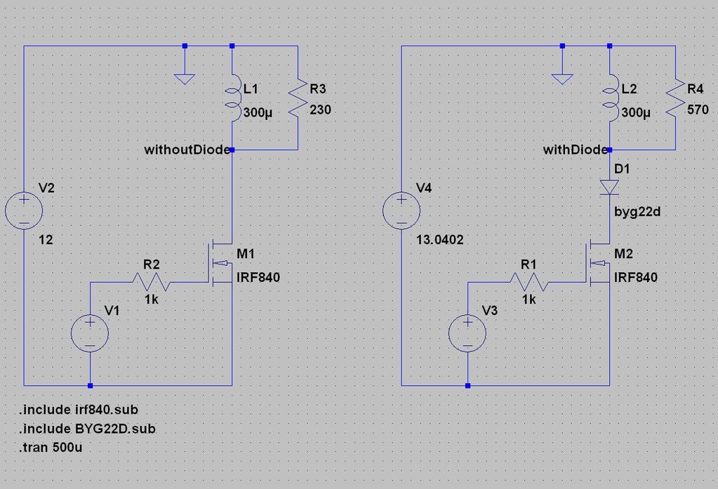
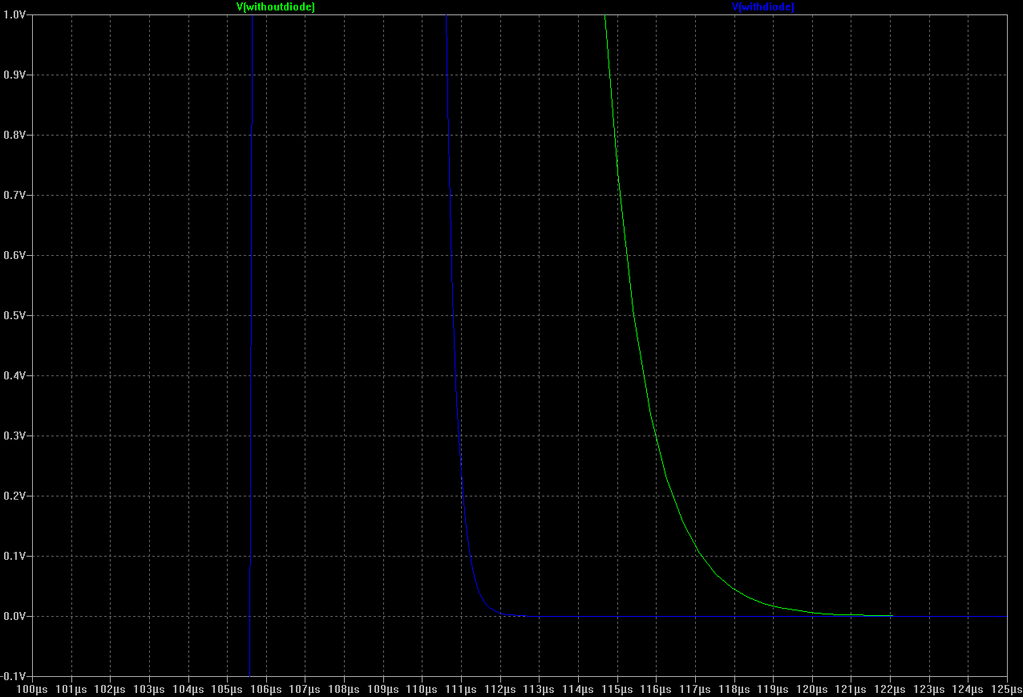
Announcement

Collapse
No announcement yet.

HH Schematic revision - thoughts?

Collapse
X
 
  • Filter
  • Time
  • Show
Clear All
new posts

  • #16
    Diode on Drain

    Originally posted by hobbes_lives View Post
    The diode capacitance is in series with the MOSFET's capacitance, so it serves to reduce the overall capacitance observed across the coil. I did some LTSpice simulations which proved the point. The simulation results held up in a circuit that I breadboarded as well. A discussion about it was held on another forum, but I can't seem to find the posts now. Aziz may recall where it was at, as I believe he was involved in the discussion as well.

    Following are the simulation circuit that I used and the resulting simulated waveforms.

    Some things to note are:
    1) I increased the voltage in the diode circuit to match the coil current in both circuits
    2) The optimum damping resistor value is much higher in the diode circuit, due to the lower overall capacitance


    On the breadboard I got a significant reduction on the delay when using the diode.
    Then I connected the scope probe to the drain and found that the transient voltage gets stuck between the mosfet and the diode, so I added a 56k resistor to drain that voltage to ground.

    So Carl is right in that the mosfet sees the same flyback voltage, however, the diode is then biased such that the drain capacitance can not go to the coil anymore.

    Tinkerer

    Comment


    • #17
      PIC timing

      Attached the PIC timing

      Tinkerer
      Attached Files

      Comment


      • #18


        I though of that too! Well sorta. I know Series Capacitance is opposite of Series Resistance in that it Reduces total Capacitance.

        I thought of adding a capacitor to the coil input to reduce over all C. With the longer Pulse withs it would become restrictive, ( Resistive ) and not work or impede the return (fly Back ) and under laying target signal.

        I did not think about the Capacitive Reactant's of Semiconductors. A transistor connected E and C would provide adjustable C if done right! Sorta like a VariCap!

        Could you bias a transister in such a way as to eliminate most of the fly back and retain the Target signal?

        Let the Capacitor Obsorb and block most of the Fly Back Current and Once the Capacitive Reactance starts to block the Fly back , take the Sample from the Coil End of the Capacitor with Reduced Power of the Fly Back?

        If not set up right, Your making a Tank Circuit and is going to Creat a Bad Ringing Set up. If you could get it Tuned Right, I would think the Target Signal would Stand out Better?

        Am I talking out my azz or what?


        For my Referances and Leaking Brain only!

        http://www.wisc-online.com/objects/i...?objID=DCE2602


        Comment


        • #19
          PIC and sine wave VCO

          Hey again, all,

          The schematic below is gettin' about close to copper, I hope. So I'm asking: any thoughts or things anyone thinks I missed?.

          I added the option of the diode/resistor/mosfet combo just to allow for playing with it. So far it looks like the jury is still out on that one.

          I also decided to just go for it and get rid of the original timing circuit.
          I've replaced the 555 clock and 74HC221's with a MicroChip PIC 16F684 and I'm starting on the code now. I should have a few sim results soon.
          The usual LCD display is conspicuously absent.
          I can tell where the knobs are set, and I really don't see the need for a redundant, power sucking LCD display that I'll hardly ever have time to
          look at (hillsides, rattlesnakes, open mine shafts, U/W, et al).

          And now for my 'odd' one,

          I really can't stand the 'growl' of a square wave VCO, so I thought I'd try something different. So... IC10, IC12, and IC13 comprise a voltage to
          frequency sine wave generator for a smoother sound (I hope).
          I've ordered the chips to test this idea out on my working HH, we'll see.

          I have no idea if the transistor pair still needs to go between the final op amp and the new VCO circuit or not. Any ideas? Thoughts?

          Anyway, here it is:

          Click image for larger version

Name:	sch3.JPG
Views:	1
Size:	205.6 KB
ID:	321304


          Input, anyone? Thanks, GTB

          Comment


          • #20
            U14

            Well, I noticed one glaring error...U14 should be at V+ for the pwr pin, not at +5vD, oops. There's probably a few more. The sine wave vco parts should be here by Sat. or Mon., we'll see how that idea works then.

            BTW, Here's the thinking on the VCO sine wave circuit:
            IC13 is a switched-capacitor lowpass filter. The clock frequency, provided by IC10, determines the filter's 3-dB corner frequency in the ratio of 100:1. Thus, the corner frequency is 100 Hz if IC13's clock frequency is 10 kHz. Meanwhile, IC12 divides the clock frequency by 64 to provide the input to IC13. Because the input frequency is higher than 1/100th of the clock frequency, only the fundamental of the square-wave input can partially pass through the filter. The fundamental passes through the filter with about an 8-dB loss. The total harmonic content is lower than 60 dB.

            That's the plan, anyway,

            Laters, GTB

            Comment


            • #21
              Driving the MOSFET

              Originally posted by GT Blocker View Post
              Well, I noticed one glaring error...U14 should be at V+ for the pwr pin, not at +5vD, oops. There's probably a few more. The sine wave vco parts should be here by Sat. or Mon., we'll see how that idea works then.

              BTW, Here's the thinking on the VCO sine wave circuit:
              IC13 is a switched-capacitor lowpass filter. The clock frequency, provided by IC10, determines the filter's 3-dB corner frequency in the ratio of 100:1. Thus, the corner frequency is 100 Hz if IC13's clock frequency is 10 kHz. Meanwhile, IC12 divides the clock frequency by 64 to provide the input to IC13. Because the input frequency is higher than 1/100th of the clock frequency, only the fundamental of the square-wave input can partially pass through the filter. The fundamental passes through the filter with about an 8-dB loss. The total harmonic content is lower than 60 dB.

              That's the plan, anyway,

              Laters, GTB
              It would be good to use a MOSFET driver to drive Q5. Much faster switching than the transistors.

              Tinkerer

              Comment


              • #22
                MOSfets

                Hey there, Tinkerer,

                Not a bad idea to try.
                I'll use TO-92 sockets to allow for some playing room with the choices on Q4 and Q3 (and SIPs for the biasing resistors).

                I also realized that I don't need the X-tal for clocking U6. I originally planned on using the output of R36 to drive an A to D pin on the pic chip for Sq wave audio out from another pin (much like the orig 555 setup). That required fast clocking on the PIC.

                Since deciding to try a separate sine wave output circuit (U10,U12/13), there isn't any reason for 20mHz clocking on the PIC.
                The LM331 should handle V:F square wave gen fine without the pwr grid spiking of the 555 (since that's what it's designed to do...). And hopefully, I got the sine wave gen circuit right*.
                That freed up a couple pins on the PIC. So...

                I've decided to add a SPDT switch between +5v and GND to IC6 pin RA5 (11) to toggle master timings between large and small coils (as to the effects of RV1-2, RV5-7. {Freq, Pulse Width, Main Delay, Sec Delay, and SecDel Width})*.

                As I get some code together, I'll post it for those following my antics.

                *ANY input is welcome (come on other guru's...)

                Thanks again for the input, Tinkerer. GTB

                Comment


                • #23
                  oops - U13 fix

                  Looks like I missed another one. Here's the fix for U13. I musta been pretty tired to forget/messup the pwr pins, duh.

                  Click image for larger version

Name:	fix.JPG
Views:	1
Size:	17.9 KB
ID:	321313

                  Hopefully, that's the last of the dumb mistakes (uh huh).

                  Comment


                  • #24
                    VCO audio

                    OK Folks,
                    I guess I really screwed up the sine wave VCO idea. I tried out the idea and it didn't work worth a ..well, you know. I the tried using the output from the HHvD1 IC9 NE555 to feed the circuit instead of the LM331. Better, but no cigar. So...scrap that idea.

                    Next I started playing with the original HH circuit with the following changes (all referenced from Carl's HHvD1 schematic):

                    I replaced R55-1k with 4.7k, replaced R39-1k with a 5k pot in series with a 4.7k to C22, and routed Q6 to IC9-pin 7 instead of pin 6. I also dropped R48 to ~1.5k, though I'm not sure if I needed to at this point.

                    The result is a smooth, stable tone that can be adjusted in pitch with the R39 5k pot replacement (the resistor in series lowers the base tone for the pot adjustment -the more k, the lower base tone at the minimums).

                    The result in the audio surprised me. It is nearly the 'sine wave' sound that I was looking for. Now I'm wondering if I have lost any audio sensitivity, and if so how to get it back.

                    More tests are needed, as usual. Hopefully someone here will give this a try so we can compare notes. It's a simple change to try.

                    I REALLY like the new audio, more like my Minelab Eureka (maybe that's why I like it?). MUCH easier on the ears. No more 'motor boat' crackling. I just hope I can tweak it to get the most out of it.

                    If anyone decides to give this a try, please post your results. I'd like to know what those of you in the the HH community think about the change and how to improve it.


                    Thanks, GTB

                    Comment


                    • #25
                      Posted the above in a seperate thread

                      Hey again,
                      I reposted the above in a new thread. I think it fits better there. Sorry if I messed up. GTB

                      Comment


                      • #26
                        hi all i has built hammer head old rev that is conect to r 31 to ground i mean 0 volt but g t bloker omited this in third gain i dont know where is wrong.........

                        Comment


                        • #27
                          You are right

                          Hey Rajesh,
                          You are right, I overlooked it or accidentally deleted that trace. Add it in, BUT DON"T try the LM331 audio circuit! It doesn't work. Use Carl's audio circuit with the NE555 as per the original HH schematic or my new mod above.
                          Laters, GTB

                          Comment


                          • #28
                            hh

                            hi GT Blocker > again
                            I know that it fits and better hh schemetic but can you send me n3 and n4 and ne555 pin no 3 frequency speed pulse width +dead time . Sorry ................

                            Comment


                            • #29
                              Originally posted by GT Blocker View Post


                              Input, anyone? Thanks, GTB
                              You should avoid using junctions on crossing wires, like for instance:
                              U1-C4-C5-R1, R32-R31-R30-C23 and so on.
                              Some pins are left unconnected like U2:A for instance, most CAD software will generate an error flag in such situations.
                              Sometimes it's better to draw the inverting input of the OPAMP on the upper part and the non-inverting lower down. While that's not critical it does improve the reading of your schematics.
                              Regards,

                              Comment


                              • #30
                                Rajesh timing Q

                                Howdy Rajesh,

                                Please understand one thing above all else in this thread:

                                My HH revision thread is NOT to intend that I have improved the HH, NOR do I think ANY modification idea that I have attempted is 'better' than Carl's original HH design.
                                Carl is working on a newer version as this is written, and I know he'll have a MUCH better design than I could ever hope to do.

                                That said, the point of this thread was to generate new ideas and tweaks for the HammerHead.

                                The schematics that I have posted are UNTRIED (other than sims up to the audio section, and that last audio mod idea), and I probably have no idea what I'm doing at that.

                                Take them with more than a grain of salt (test the ideas first...).

                                Anyway, to get to your question:

                                As far as the timings go, look in this thread at post No.79:
                                http://thunting.com/geotech/forums/s...t=14001&page=4

                                The code is not for a MicroChip PIC, but if you can program a microcontroller it should make sense to you.
                                Good luck! GTB

                                Comment

                                Working...
                                X