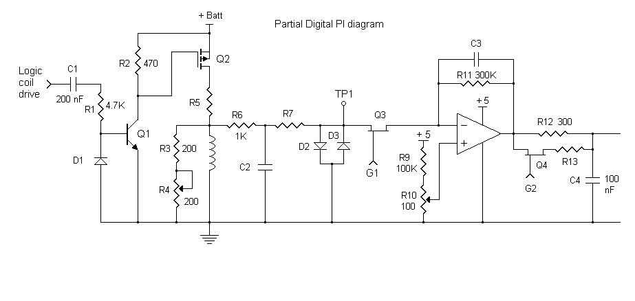
I have combined some of the pieces of the design I have been working on.
C1, R1, and D1 provide AC coupling so the coil current will not get stuck on if the software forgets to turn the coil drive signal off.
Q1 and R2 provide level shifting to drive the power FET Q2 which turns the coil on and off.
R5 is a current limiting resistor which may be 0.
R3 and R4 are the damping resistance.
R6 is the input resistor of the amplifier and is one of the components that determines the amplifier gain.
R7 and C2 are optional components for RF filtering. R7 would be smaller than R6 or it might be replaced by a ferrite bead filter.
D2 and D3 are the clamping diodes that protect the amplifier from high voltages during the coil on-time and flyback.
Q3 is still up in the air. This could be used to gate the amplifier. Or I might replace it with a resistor or diode or nothing.
R9 and R10 are the offset adjustment for the amplifier.
R11 is the feedback resistor for the amplifier and along with R6 determines the gain.
C3 is the feedback capacitor which sets the bandwidth of the amplifier. If it is used at all it will probably be set to a time constant of a few usec.
R12, R13, C4 and Q4 form a variable time constant filter. R13 will be smaller than R12 and might not be necessary at all if Q4 has the right on resistance. normally Q4 will be on, providing a low resistance path to C4. The time constant should be a few usec. To switch to lower bandwidth, Q4 is turned off, then R12 and C4 make a longer time constant filter, about 30 usec. There should not be much of a transient when Q4 turns off.
The output of this section goes into the A-D converter.
Robert
