If this is your first visit, be sure to
check out the FAQ by clicking the
link above. You may have to register
before you can post: click the register link above to proceed. To start viewing messages,
select the forum that you want to visit from the selection below.
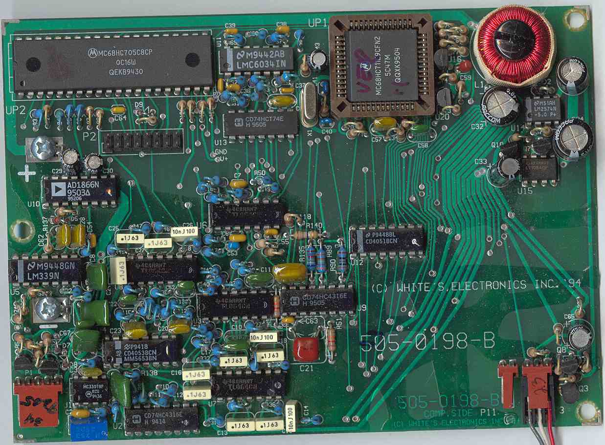
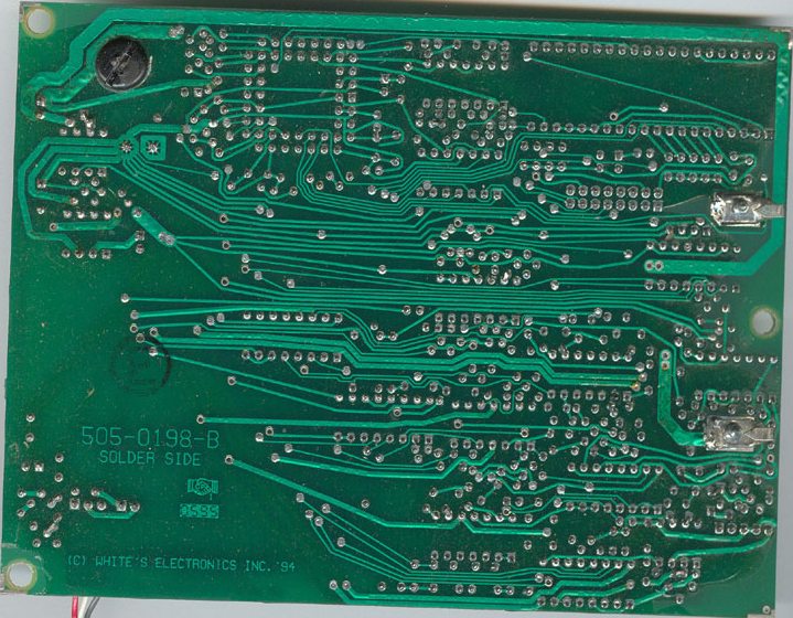
Can you scan and post the other side of the PCB as well. Interesting to see how White design & route their PCB boards. My first impression of the PCB design (track routing) is very unprofessional made. But to get a better view over the design I need to see the other side of the PCB (solder side).
thanks for the scan. I expected such a layout as I saw the component side of the PCB.
@ Sean yes, star grounding is good but too much of star grounding is not good. Only certain parts of the ground net need to be routed as star grounding. The rest is not necessary. And look at all the tracks...ugly routed with too much corners and not smooth (look at Carl's PCB and compare). That's a much better PCB.... The XLT PCB is not a good EMF designed PCB. At each corner of the PCB track EMF escape. No ground planes (grid) and the big track on top (see solder side) is to small. The track is over heated....you can see a melted tinned track under the solder mask. I'm really disappointed to see such PCB's design from an established company like White's Electronic. If I look back to the late 80's my DIY-PCB's made in the garage looked much better in design than this one.
I think opposite. I think it is good layout, as for two-layer PCB.
The PCB design is sometimes kind of black magic and odd looking design is a result of trial and error process. I think this is an example of a good working detector so one can learn from such design, not from a text book.
The Carl's design looks worse for me (sorry Carl - you did a great work anyway, besides I am not an expert to criticise). I do not understand why you refer to it, Chris - I can see more corners than in White's and the power part is not separated from the rest of the electronics. I hope it works well without lock-ups.
Ground plane is very good option for multilayer PCB. One layer for ground only, that's the best option (with or without a grid).
Also the "over heat" has definitely occurred while the board has been soldering - not caused by current!
That is my two-cent worth comments - I do not want to start a wrangle here and not to offence anyone. Just wanted to say I like the PCB routing !
Ha! Thanks a lot Piotr! Just kidding, even I'm not satisfied with my PCB. IMO, single-sided boards will always be a compromise, and rarely be very good. I have plans to do a 2-sided board, using SMD, if I can ever get around to it.
I can't see the link for Carl's PCB, but if I know Carl, it will be a good one!
Only the Analogue portion should be star grounded, the digital should use a "rail" system which should then be terminated at the star point via a ferrite bead or some such item.
The corners of the digital lines should be as round as possisble, but mostly you can get away with 45 degree corners. The analogue should be smooth curves.
Another thing, though not strictly neccessary at the frequencies involved in the XLT (either analogue OR digital) is to impedance match the signal lines. If this is done correctly then there should be NO leakage at all.
Burying the digital lines in between a top and bottom ground plane would also help, as would alternating signal and ground lines (next to each other) where any appreciable length of track run occurs.
Building the analogue section and the digital section on different areas of the board and using screening cans would be another help.
As I am used to working in the GHz range of frequencies on military equipment, I am well aware of the valid points you are making. The only factor is the cost involved when you go to multi layer boards, especially if you use a low hygroscopic substrate like F4.
The track on the XLT is not overheated. When they manufacture the boards, they use HOT TINNING as opposed to electro tinning. The Whites board clearly shows this. The boards are then etch resist on after.
 Tweet
Tweet

Comment