Announcement

Collapse
No announcement yet.

H BRIDGE DRIVER

Collapse
X
 
  • Filter
  • Time
  • Show
Clear All
new posts

  • H BRIDGE DRIVER


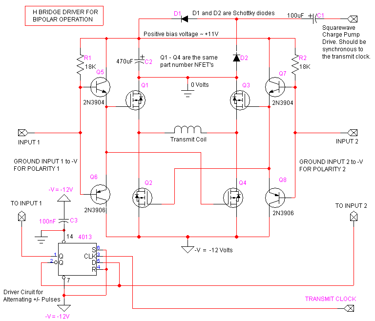
    Here is the schematic for an H bridge which uses all N channel FET's. High side drive switching is made possible by the use of a charge pump which provides an extra positive supply. I used the transmit timing square wave to drive the charge pump. A 555 has no trouble driving it. I used a separate receive coil but it should be easy to run into a standard coil amplifier circuit.

  • #2
    Re: H BRIDGE DRIVER

    Looking at a half-circuit consisting of Q1 & Q4, I think Q1 needs to be left on during flyback, so that the coil will decay to the same level (ground) every time. So I would need to clock Q1 seperately. Also, I assume the inputs would have to be from open-collector-type drivers, in order for the 18k pullups to work.

    At the same time, Q2 & Q3 should be off, and in no way affect the impulse, except for minor capacitive loading. But the internal diode of Q3 will turn on with a positive flyback, and kill the signal. I saw this when I tried an all-NMOS configuration some time ago. Also saw it when using PMOS for Q1/Q3, but in that case, it was simply the flyback turning on the PMOS via Vgd.

    So I tried putting series diodes on the top-side MOS drains, so the flyback would see a high-threshold reverse diode. This does keep the MOS from turning on, but completely screws up the return decay level. Everything just bounces all over the place. However, looking at this circuit again made me think, what if I resistively bias those diodes all the time? The resistors will look like part of the damping R, and the return decay level should clean up.

    I'll give it a try...

    --Carl

    Comment

    Working...
    X