Announcement

Collapse
No announcement yet.

Partial digital PI design

Collapse
X
 
  • Filter
  • Time
  • Show
Clear All
new posts

  • Partial digital PI design


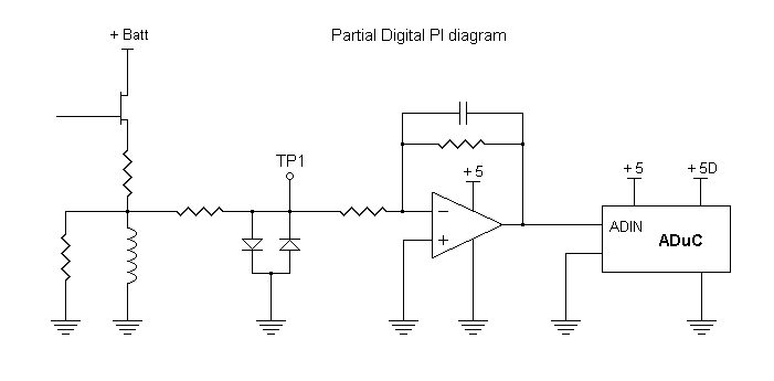
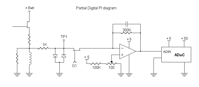
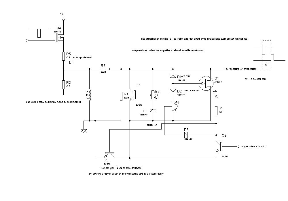
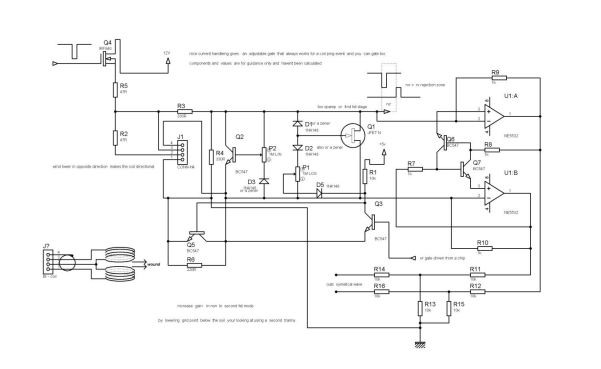
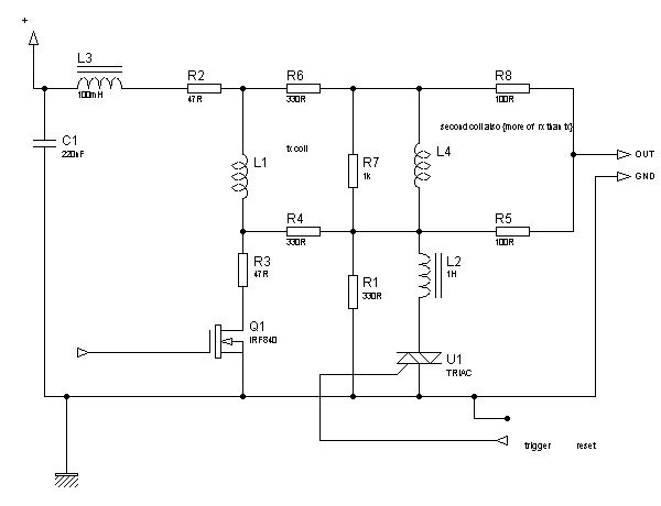
    I am going to start designing a digital PI board. This is a partial diagram showing the area I am concerned about now.

    Starting at the back end and working toward the front, the ADuC microconverter runs from a single 5V supply. The analog input range is 0 to 2.5 volts, but the input can go up to 5V without damage. With this narrow input range I do not see any point in having a wide output swing from the amplifier. I would just have to clamp the voltage to the allowed AD input range anyway. So I would prefer an amplifier that runs off a single 5V supply and which allows the input voltage to go below the negative supply rail. With this amplifier configuration it makes sense to connect one side of the coil to ground.

    During the coil on-time the coil voltage will be positive and may go as high as the + battery voltage. During the flyback time the coil voltage will go below ground by a couple hundred volts. During the off-time the signal will be below ground but should be within a few hundred micro volts of ground.

    At TP1 the signal is clamped to within +/- one diode drop of ground. So during the coil on-time the voltage will be +1 diode drop. During the flyback it will be -1 diode drop. And during the off-time will be within a few hundred micro volts of 0.

    I am looking for an amplifier with the following characteristics:
    - single 5V supply
    - allows inputs below - supply
    - can provide single stage gain of 300
    - has gain bandwidth product greater than 6 MHz
    - has reasonably low noise

    I am looking at the AD8031 for the amplifier. These are the things I am worried about:

    1. During flyback TP1 goes below 0. The output of the amplifier can only go up to 5 volts. So the -input of the amplifier may go below -0.5 volts. This is the limit of the AD8031 linear range. I do not know what the amplifier will do in that case or how well it will recover.

    2. The gain is high enough that the input offset current will be a problem and the amplifier does not have an offset adjustment. This means an offset adjustment should be added to the amplifier input.

    3. The AD8031 noise figure is not as low as I would like. It is about 4 times higher than the 5534. But the amplifier noise will still be way below the external noise.

    4. During the off-time the target signal will be negative but noise can make TP1 go positive. This will cause the amplifier output to hit 0 and cause a bias in the AD samples. It would make sense to bias the amplifier +input a bit above ground, but this makes point 1 worse. Maybe if I bias it only a mV or so this will take care of this point and point 2.

    I would appreciate any suggestions.

    Robert

  • #2
    Re: Partial digital PI design


    i solved this problem using active blanking and some extra fet s a switches
    simply removing the diodes out the equassion

    so now you get a nice voltage swing you can set a max amout too with a pot

    here is a jpeg to show this stage and its switches

    Comment


    • #3
      Re: Partial digital PI design

      also this design doubles as an ib type pi for depth of find

      Comment


      • #4
        Re: Partial digital PI design

        I have thought about gating the signal, and that is something I will still consider. One consideration though is that I want to keep the parts count low. I would like one version of this to fit inside an electronic probe on a board about 20 mm x 80 mm or about 0.8 x 3 inches.

        Robert

        Comment


        • #5
          Re: Partial digital PI design

          use a differential ampilfier taking the two signals via diodes in series {use germanium to give a higher voltage you want...}

          Comment


          • #6
            Update


            I have modified the design a little.

            I added an offset adjustment for the amplifier that will allow the amplifier output to be set a couple hundred millivolts above ground. That should provide room for offset and noise and drift.

            I also added a FET so the amplifier can be disconnected during the coil on-time and flyback. There are two reasons I would like to do that. One is to protect the amplifier input from going too far below the negative supply during the flyback. The other reason is that I would like to be able to reduce the amplifier bandwidth for long time constant targets. I have not shown how that would be done yet. This would be for use with long sample delays where the short time constant signals are not going to be detected anyway. The narrower bandwidth would reduce noise. The problem with less bandwidth is that the amplifier would not recover from the flyback pulse in time. The gate keeps the flyback pulse out of the amplifier so it does not need time to recover.

            The timing sequence for short sample delays would be: turn coil drive off, wait a few usec for the field to collapse, turn the wide band amplifier on, wait for it to settle, take first sample. The timing sequence for long sample delays would be the same until the amplifier settles, then the amplifier would be switched to narrow band and after a longer delay the first sample would be taken. By wide band and narrow band I mean roughly 20 kHz and 5 kHz.

            I need to find a low current FET that will be off when the gate is 1V above the source and on when the gate is 4 volts above the source.

            Robert

            Comment


            • #7
              Re: Partial digital PI design


              hi robert
              take a look at this little bmp

              then you can tune some more bits and dispense with the shunt recifier leaving the signal path clear

              but also gate the even to a second fet follower type amplifier

              i used a buk device {made for pwm}

              also a simple npn switch for the voltage peek
              {after the shunt resistors on the coil the voltage wont be much

              as a 1n4148 is only 50 v piv so.....


              a transisotor alone is fine

              to shunt away and ht
              and also give resample gateing

              Comment


              • #8
                Re: Partial digital PI design

                i think this could be easy

                what you need man is the circuits and data for
                coin acceptors

                these use pwm analysis technique
                and are very sofisticated to prevent fraud

                they measure relative flux density of the metal these tables are known
                and a point
                can carl please publish a set of relative permiable flux density of known metals and salts


                tables for known types i think these table are easy too find

                perhaps if i can find a link
                so perhaps i think you could use a ferrite core but you need to shape it as a flat H shape
                with four balanced radiators each a 1/4 wave at i will mail details

                i will mail you a site i use for these calculations and a method to do them for such a small coil using fine wires {gives all factors easy.....}

                let me mail

                Comment


                • #9
                  Re: Update


                  here is another

                  added feature i bet you didnt think of

                  .....

                  Comment


                  • #10
                    Re: Update

                    you may need a resistor across the gnd coupler tranny
                    say what 330R good alround value
                    and my best value left now from the last few bags of 1000s types

                    i think if your making small this is a nice way to solve the problem just one more micro pin and no real hastle

                    the directional coil is a nice feature in a tube
                    but if it has to be omni and a probe them hum ..... you need to use a coil loops rather than one

                    what i would do personaly is take a coil say 20T 20T .71 mm or 17T 17T .51

                    at say 19 cm

                    center tap wind in opposite from the tap onward and also turn the coil to a figue 8 then loop it and fold down the middle
                    dont use tape on enamaled wire you dont need it wind it as a whole .. then tap as a bullet....
                    leaving the wires at one end

                    very neatly

                    tell me if i am not helping and ill go away

                    as for the opamp i think your choices of next stage are good

                    the blanker shunt follower will work but ??maybee.... a dual coil is good also and auto switch for main voltage disgarde the crap 1n4148 noise gens...

                    try this take a 10khz signal and rectify it with a shunt {use audio} then youll see that it sounds like shuuuuuuuuuuuuuuuuuu marbles in a tube instead os nothing but a voltage increase

                    Comment


                    • #11
                      Re: Update


                      a more explicit version

                      Comment


                      • #12
                        Re: Update


                        here is a triac version

                        values are for guidance not real ones

                        not any accuricy mearly the idea as a circuit form

                        Comment


                        • #13
                          Re: Update


                          here is another good extra too add

                          Comment


                          • #14
                            Re: Update


                            and another way to maximise recieve surface areas

                            Comment


                            • #15
                              Re: Partial digital PI design

                              I tend to prefer designs that use only enough parts to get the job done.

                              I used two clamp diodes to provide protection for the op-amp. There might be more complicated ways to accomplish the same thing, but this simple method seem to work adequately in other designs.

                              The purpose of the FET is to keep the on-time and flyback pulses out of the amplifier so I can play around with narrow bandwidth. Either a series or shunt FET could be used. There are some potential problems with the design I showed. I am trying to get by with only a +5 volt supply. This means that I only have a 5 volt logic swing available to switch the FET. I need a minimum Vgs that is greater than one diode drop and a maximum Vgs of about 4V. Also during the on-time the source will be about a diode drop higher than the drain. The FET has to remain off when this happens, so it cannot have a built in clamp diode. But what is worrying me the most is the possibility of noise getting into the input of the amplifier. The output pins from the CPU have low level noise on them. I am afraid that some of this noise may get through the FET and into the amplifier. Since I want to achieve a sensitivity around one microvolt it would not take much noise to cause trouble. So I am thinking about removing the FET. Instead I would put a switchable filter after the amplifier. The signal is larger there and will not be as sensitive to noise. In that case the amplifier bandwidth would stay the same but there would be a 30 usec RC filter between the amp and the AD that can be switched out.

                              Robert

                              Comment

                              Working...