
 Tweet
Tweet
Hi master;
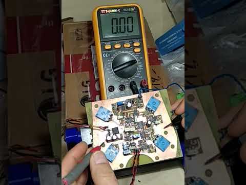
I measured the supply voltages.
I did not take any other action.
I will act according to the answer from you.
I am aware you are angry but sorry.

I measured the supply voltages.
I did not take any other action.
I will act according to the answer from you.
I am aware you are angry but sorry.

Comment